
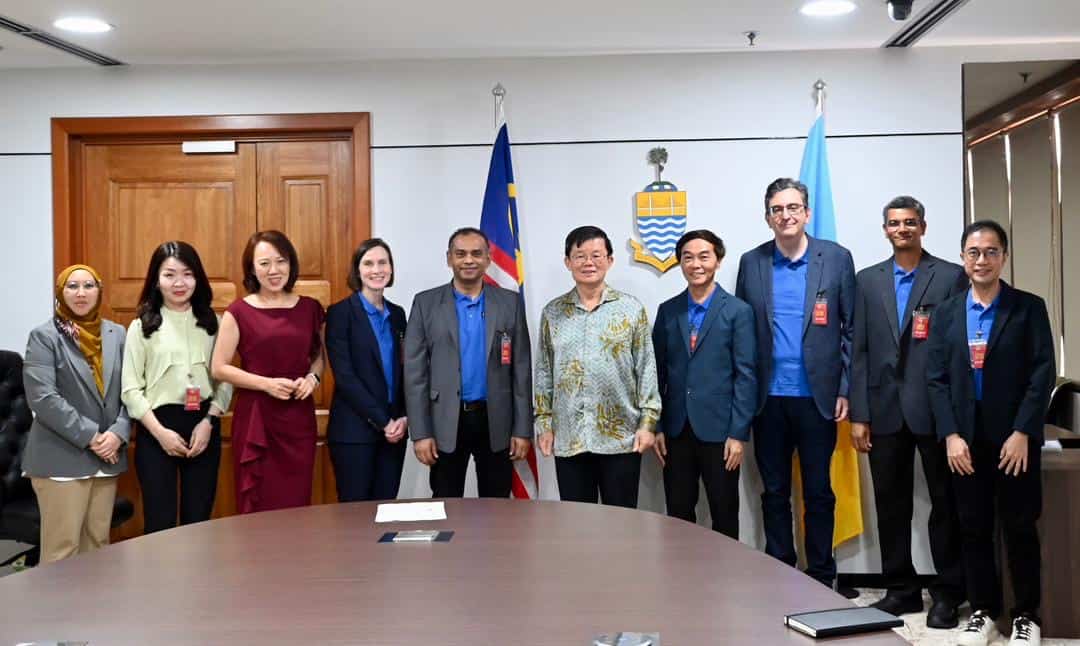
PENANG took another step in strengthening its global technology partnerships today when a delegation from Microsoft paid a courtesy visit to Chief Minister Chow Kon Yeow at his office in Komtar, underscoring growing international interest in the state’s thriving semiconductor ecosystem.
During the meeting, InvestPenang chief executive officer Datuk Loo Lee Lian highlighted Penang’s strong position in the global integrated circuit (IC) design landscape, noting that the state has built one of the region’s most concentrated clusters of chip design talent.
“Penang today has the highest concentration of IC design and related companies in the region, and this talent pool began more than 20 years ago from the IC design division of Intel.
“We are now expanding this foundation through our ‘Penang Silicon Design @ 5KM+’ initiative to make the ecosystem even more collaborative and future-ready,” she said.
Loo explained that the initiative integrates purpose-built hybrid workspaces and labs, talent development programmes and startup incubation into a tightly connected innovation cluster.
Nearly one million square feet of specialised facilities have already been developed to support chip design activities, while the Penang Chip Design Academy run by the Penang Skill Development Centre is retraining graduates and upskilling engineers to meet industry demand.
“We are growing a sustainable local pipeline of talent and supporting homegrown startups with training, shared tools and incubation space.
“At the same time, we welcome global partners to collaborate with us and help shape future skills development,” she added.
Microsoft’s Silicon, Cloud Hardware, and Infrastructure Engineering Organisation corporate vice-president Reynold D’Sa said the state’s efforts strongly align with the company’s direction as silicon increasingly powers cloud computing and hyperscale systems.
“In the past decade, we have moved more towards the cloud that uses silicon at a massive scale.
“Designing silicon in the context of the larger system is now extremely important to get the most value from it.
“Understanding high-volume manufacturing and global operating environments is critical as products are deployed across different climates and use cases worldwide,” he said.
Reynold also stressed that artificial intelligence is rapidly reshaping both semiconductor design and manufacturing.
“The way students learn today is already changing. Traditional IC design is becoming very different because AI is transforming how we design, analyse data and improve productivity and quality.
“We are excited to see the work being done here and look forward to exploring how we can grow teams and adapt to the new AI workforce,” he further commented.
Also present at the meeting were Microsoft Silicon Engineering corporate vice-president Selim Bilgin, MSFT site lead Siew Beng Thum, partner Sriram Srinivasan, senior director Terrence Tan, and Reynold’s chief of staff, Jennifer Wickham.
Story by Kevin Vimal
Pix by Alissala Thian