

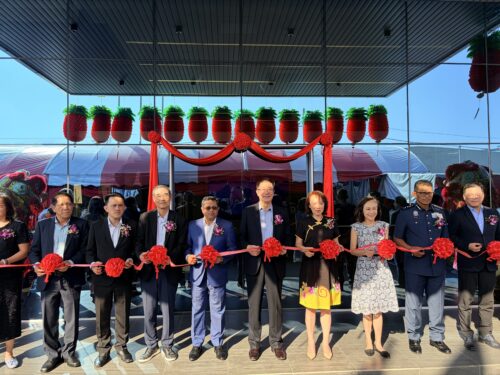
A LEADING global provider of semiconductor packaging and testing services, Chipbond Technology Corporation, through its Malaysian subsidiary Chipbond Technology Malaysia Sdn Bhd, officially opened its new advanced manufacturing facility at Valdor Industrial Park in Batu Kawan today.
The establishment of the facility marks a significant milestone in Chipbond’s global expansion strategy, with a total investment of nearly US$200 million (approximately RM800 million).
The new plant further strengthens Malaysia’s position in the global outsourced semiconductor assembly and test (OSAT) value chain, while reinforcing the country’s role as a key hub for advanced semiconductor manufacturing.
Malaysian Investment Development Authority (MIDA) chief executive officer Datuk Sikh Shamsul Ibrahim Sikh Abdul Majid, who attended the opening ceremony, said the facility represents a major new investment that expands Malaysia’s OSAT capacity and ecosystem, while enhancing the nation’s overall semiconductor competitiveness.
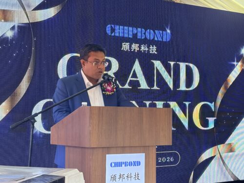
“It brings deeper integration, technology transfer and the development of local capabilities that will benefit Malaysia’s semiconductor ecosystem for years to come.
“Chipbond is introducing advanced OSAT expertise in wafer bumping and chip-scale packaging, which requires highly skilled engineers.
“Through structured training programmes and university collaborations, Malaysians will be equipped with the skills needed for complex, high-value semiconductor production.
“With companies like Chipbond anchoring advanced capabilities here, Malaysia is building an integrated semiconductor ecosystem where local talent and small and medium enterprises (SMEs) can participate meaningfully in global value chains,” he said.
Meanwhile, InvestPenang chief executive officer Datuk Loo Lee Lian noted that backed by more than five decades of industrialisation and a strong OSAT foundation, Penang has developed a mature ecosystem, a skilled talent pool and a highly conducive business environment.
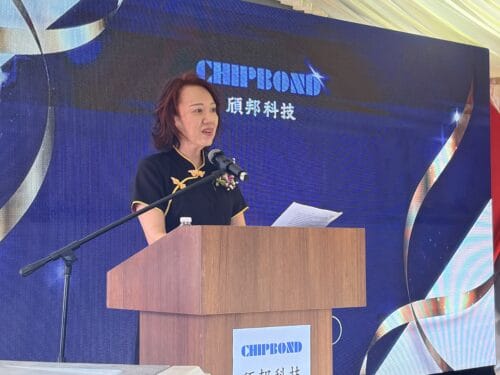
“Investments such as Chipbond’s are strategic in driving Penang’s shift towards advanced packaging and innovation-led growth, in line with the National Semiconductor Strategy (NSS).
“We look forward to strong knowledge transfer, talent upskilling and deeper collaboration, which will further strengthen Penang’s position as a regional hub for advanced semiconductor packaging,” she said.
Chipbond chairman Wu Fei Jain emphasised that the new facility underscores the company’s commitment to expanding its global footprint while ensuring a stable and continuous supply for customers.
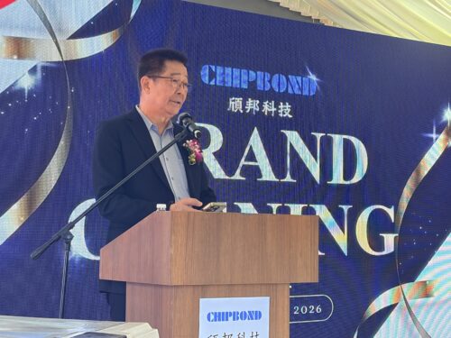
“Without the support of the Malaysian government, the contributions of our customers, and the tireless dedication of the Chipbond team, we would not have been able to achieve this ambitious goal within such a compressed timeframe,” he said.
It is understood that the Penang facility will offer advanced semiconductor processes, including wafer bumping, wafer-level chip-scale packaging (WLSP) and testing, with an initial capacity of 10,000 wafers and 100 million WLSP units per month.
The plant is also equipped to support flip-chip packaging assembly and testing, providing flexibility to meet future technological advancements and customer demands.
Also present at the ceremony were Bukit Tambun assemblyman Goh Choon Aik and Penang MIDA director Muhammad Ghaddaffi Sardar Mohamed.
Story by Riadz Akmal
Pix by Noor Siti Nabilah Noorazis